'Impossible' conductivity explained
18 Jun 2010
Bring two materials that are not themselves conductive into contact and, exactly at their interface, something remarkable happens: at that precise point, conduction is possible.
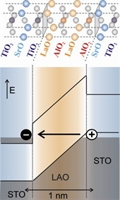 |
| In a stacked atomic structure of lanthanum oxide with a strontium titanate capping layer on a substrate of strontium titanate (crystal structure from left to right, top of illustration), the internal potential in the LAO layer brings about a redivision of charge. The resulting electrons on the interface leave behind holes that are just one nanometre apart. The electrons (left) and gaps (right) in parallel produce a contribution to the electrical conductivity. |
That is not only a breakthrough in our understanding of the phenomenon, it also opens up possibilities for new forms of nanoelectronics. The researchers have published their findings in Physical Review Letters.
The researchers from the University of Twente had earlier demonstrated that two non-conductive metal oxides could become conductive at the exact point where they come into contact, and that non-magnetic metal oxides 'suddenly' become magnetic at their interface, for example in the combination of strontium titanate and lanthanum aluminate. When these two complex oxides come into contact, various ions are present on both crystal interfaces, all with their own charges. When the two oxides come into contact, a rearrangement of the charge, known as electronic reconstruction, takes place.
At the point where the electrons are more numerous, these electrons can now conduct electricity. At the same time, it would be expected that holes - positive charge carriers - would be created elsewhere in the structure, where the original electrons were located. The new calculations and experiments have now shown that these holes do indeed exist, and that the holes and the electrons move in parallel to each other, with a space of just one nanometre between them. This is not only a breakthrough in the understanding of conduction at the interface, it also opens up the way for new applications that are not yet possible in current semi-conductor electronics. One exciting possibility, for example, is that interaction might also occur in these conductive layers, which are so close together, with new particles and quantum states as a result.
One unit cell is enough
What is more, until now it was assumed that oxides with a specific thickness were needed to achieve this effect. However, the newly published research shows that the mechanism occurs even with a thickness of a single unit cell: just one layer in the crystal. The MESA+ Institute for Nanotechnology has unique facilities for building up these types of oxides atomic layer by atomic layer, and in this way creating materials with an astonishingly wide range of properties.
The new results were achieved by a large international research team. As well as Munich, Davis and Berkeley, four MESA+ research groups were involved: Inorganic Materials Science, NanoElectronic Materials, Physical Aspects of Nanoelectronics and Interfaces and Correlated Electron Systems. The research was funded from the Netherlands by FOM, NWO, VIDI and VICI grants and NANONED.
.............................................................................................................................................
The article Parallel Electron-Hole Bilayer Conductivity from Electronic Interface Reconstruction, by R. Pentcheva (Munich), M. Huijben (MESA+), K. Otte (Munich), W. E. Pickett (Davis), J. E. Kleibeuker (MESA+), J. Huijben (MESA+), H. Boschker (MESA+), D. Kockmann (MESA+), W. Siemons (Berkeley), G. Koster (MESA+), H. J. W. Zandvliet (MESA+), G. Rijnders (MESA+), D. H. A. Blank (MESA+), H. Hilgenkamp (MESA+) and A. Brinkman (MESA+) has already been published online on the website of Physical Review Letters and will soon appear in print.