Patterning defect-free nanocrystal films with nanometer resolution
By By David L. Chandler, MIT News Office | 22 Aug 2012
 Films made of semiconductor nanocrystals - tiny crystals measuring just a few billionths of a metre across - are seen as a promising new material for a wide range of applications. Nanocrystals could be used in electronic or photonic circuits, detectors for biomolecules, or the glowing pixels on high-resolution display screens. They also hold promise for more efficient solar cells.
The size of a semiconductor nanocrystal determines its electrical and optical properties. But it's very hard to control the placement of nanocrystals on a surface in order to make structurally uniform films. Typical nanocrystal films also have cracks that limit their usefulness and make it impossible to measure the fundamental properties of these materials.
Now, researchers at MIT say they have found ways of making defect-free patterns of nanocrystal films where the shape and position of the films are controlled with nanoscale resolution, potentially opening up a significant area for research and possible new applications.
''We've been trying to understand how electrons move in arrays of these nanocrystals,'' which has been difficult with limited control over the formation of the arrays, says physicist Marc Kastner, the Donner Professor of Science, dean of MIT's School of Science and senior author of a paper published online in the journal Nano Letters.
The work builds on research by Moungi Bawendi, the Lester Wolfe Professor of Chemistry at MIT and a co-author of this paper, who was one of the first researchers to precisely control nanocrystal production. Such control made it possible, among other things, to produce materials that glow, or fluoresce, in a range of different colors based on their sizes - even though they are all made of the same material.
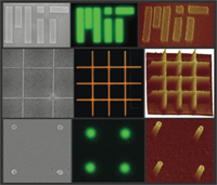
In the initial phases of the new work, postdoc Tamar Mentzel produced nanoscale patterns that emit invisible infrared light. But working on such systems is tedious, since each fine-tuning has to be checked using time-consuming electron microscopy. So when Mentzel succeeded in getting semiconductor nanocrystal patterns to glow with visible light, making them visible through an optical microscope, it meant that the team could greatly speed the development of the new technology. ''Even though the nanoscale patterns are below the resolution limit of the optical microscope, the nanocrystals act as a light source, rendering them visible,'' Mentzel says.