Materials for first optical fibres with high-speed electronic function developed
09 Feb 2012
For the first time, a group of chemists, physicists, and engineers have developed crystalline materials that allow an optical fibre to have integrated, high-speed electronic functions.
The potential applications of such optical fibres include improved telecommunications and other hybrid optical and electronic technologies, improved laser technology, and more-accurate remote-sensing devices.
The research was initiated by Rongrui He, a postdoctoral researcher in the Department of Chemistry at Penn State University. The international team, led by John Badding, a professor of chemistry at Penn State, will publish its findings in the journal Nature Photonics.
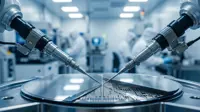
Badding and his team built an optical fibre with a high-speed electronic junction - the active boundary where all the electronic action takes place -- integrated adjacent to the light-guiding fibre core. Light pulses (white spheres) traveling down the fibre can be converted to electrical signals (square wave) inside the fibre by the junction. The potential applications of such optical fibre include improved telecommunications and other hybrid optical and electronic technologies and improved laser technology. Credit: Badding lab, Penn State University
The integration of optical fibres and chips is difficult for many reasons. First, fibres are round and cylindrical, while chips are flat, so simply shaping the connection between the two is a challenge. Another challenge is the alignment of pieces that are so small. "An optical fibre is 10 times smaller than the width of a human hair. On top of that, there are light-guiding pathways that are built onto chips that are even smaller than the fibre by as much as 100 times," Badding said. "So imagine just trying to line those two devices up. That feat is a big challenge for today's technology."
To address these challenges, the team members took a different approach. Rather than merge a flat chip with a round optical fiber, they found a way to build a new kind of optical fibre with its own integrated electronic component, thereby bypassing the need to integrate fiber-optics onto a chip. To do this, they used high-pressure chemistry techniques to deposit semiconducting materials directly, layer by layer, into tiny holes in optical fibers.