Building chips from collapsing nanopillars
By By Larry Hardesty, MIT News Office | 07 Sep 2011
The manufacture of nanoscale devices - the transistors in computer chips, the optics in communications chips, the mechanical systems in biosensors and in microfluidic and micromirror chips - still depends overwhelmingly on a technique known as photolithography.
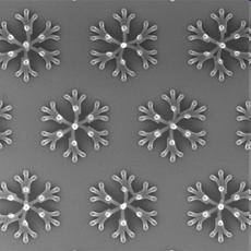 |
| Controlling the collapse of tiny pillars deposited on a silicon substrate can produce intricate patterns. |
In a pair of recent papers, researchers at MIT's Research Laboratory of Electronics and Singapore's Engineering Agency for Science, Technology and Research (A*STAR) have demonstrated a new technique that could produce chip features only 10 nanometers - or about 30 atoms - across.
The researchers use existing methods to deposit narrow pillars of plastic on a chip's surface; then they cause the pillars to collapse in predetermined directions, covering the chip with intricate patterns.
Ironically, the work was an offshoot of research attempting to prevent the collapse of nanopillars. ''Collapse of structures is one of the major problems that lithography down at the 10-nanometer level will face,'' says Karl Berggren, the Emanuel E. Landsman (1958) associate professor of electrical engineering and computer science, who led the new work.
''Structurally, these things are not as rigid at that length scale. It's more like trying to get a hair to stand up. It just wants to flop over.'' Berggren and his colleagues were puzzling over the problem when, he says, it occurred to them that ''if we can't end up beating it, maybe we can use it.''
Status quo
With photolithography, chips are built up in layers, and after each layer is deposited, it's covered with a light-sensitive material called a resist. Light shining through an intricately patterned stencil - called a mask - exposes parts of the resist but not others, much the way light shining through a photographic negative exposes photo paper. The exposed parts of the resist harden, and the rest is removed. The part of the chip unprotected by the resist is then etched away, usually by an acid or plasma; the remaining resist is removed; and the whole process is repeated.
The size of the features etched into the chip is constrained, however, by the wavelength of light used, and chipmakers are already butting up against the limits of visible light. One possible alternative is using narrowly focused beams of electrons - or e-beams - to expose the resist. But e-beams don't expose the entire chip at once, the way light does; instead, they have to scan across the surface of the chip a row at a time. That makes e-beam lithography much less efficient than photolithography.
Etching a pillar into the resist, on the other hand, requires focusing an e-beam on only a single spot. Scattering sparse pillars across the chip and allowing them to collapse into more complex patterns could thus increase the efficiency of e-beam lithography.