European collaboration's breakthrough in developing graphene
30 Jan 2010
Researchers across Europe, including the UK's National Physical Laboratory, have demonstrated how an incredible material, graphene, could hold the key to the future of high-speed electronics, such as micro-chips and touchscreen technology.
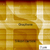 |
| Graphene, only one atom thick, climbs terraces on the surface of a silicone carbide substrate. This picture of a graphene device was taken with an atomic force microscope by Dr Olga Kazakova from the UK's National Physical Laboratory |
A paper published in Nature Nanotechnology explains how researchers have, for the first time, produced graphene to a size and quality where it can be practically developed and successfully measured its electrical characteristics. These significant breakthroughs overcome two of the biggest barriers to scaling up the technology.
A technology for the future
Graphene is a relatively new form of carbon made up of a single layer of atoms arranged in a honeycomb shaped lattice. Despite being one atom thick and chemically simple, graphene is extremely strong and highly conductive, making it ideal for high-speed electronics, photonics and beyond.
Graphene is a strong candidate to replace semiconductor chips. Moore's Law observes that the density of transistors on an integrated circuit doubles every two years, but silicon and other existing transistor materials are thought to be close to the minimum size where they can remain effective. Graphene transistors can potentially run at faster speeds and cope with higher temperatures. Graphene could be the solution to ensuring computing technology to continue to grow in power whilst shrinking in size, extending the life of Moore's law by many years.
Large microchip manufacturers, such as IBM and Intel, have openly expressed interest in the potential of graphene as a material on which future computing could be based.











.webp)


