The power of hidden patterns
By By David L. Chandler | MIT News Office | 05 Sep 2014
Patterned surfaces are all the rage among researchers seeking to induce surfaces to repel water or adhere to other things, or to modify materials' electrical properties.
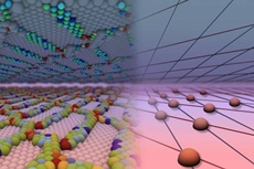 | |
| Interfaces between solid materials are surfaces with intricate, internal structure (shown on the left). To control that structure, and to use it for specific applications, researchers model it a simplified way (shown on the right).Image: Niaz Abdolrahim and Jose-Luis Olivares/MIT |
Now materials scientists at MIT have added a new wrinkle to research on the patterning of surfaces - while most research has focused on patterns on the outer surfaces of materials, Michael Demkowicz and his team in MIT's Department of Materials Science and Engineering (DMSE) have begun to explore the effects of patterned surfaces deep within materials - specifically, at the interfaces between layers of crystalline materials.
Their results, published in the journal Scientific Reports, show that such control of internal patterns can lead to significant improvements in the performance of the resulting materials.
Demkowicz explains that much research has aimed to create layered composites with desired strength, flexibility, or resistance to vibrations, temperature changes, or radiation. But actually controlling the surfaces where two materials meet within a composite is a tricky process.
''People don't think of them as surfaces,'' says Demkowicz, an associate professor in DMSE. ''If they do, they think of it as a uniform surface, but as it turns out, most interfaces are not uniform.''
To control the properties of these materials, it is essential to understand and direct these nonuniform interfaces, Demkowicz says. He and his team have taken classical equations used to describe average properties of surfaces and adapted them to instead describe variations in these surfaces ''location by location. That's not easy to do experimentally, but we can do that directly in our computer simulations.''
The ability to simulate, and then control, how defects or variations are distributed at these interfaces could be useful for a range of applications, he says. For example, in materials used on the interior walls of fusion power reactors, such patterning could make a big difference in durability under extreme conditions.
As metal walls in these reactors are bombarded by alpha particles - the nuclei of helium atoms - from the fusion reaction, these particles embed themselves and form tiny helium bubbles, which over time can weaken the material and cause it to fail.
''It's the most extreme of extreme environments,'' Demkowicz says. But by controlling the patterning within the material so that the bubbles line up and form a channel, the helium could simply diffuse out of the materials instead of accumulating, he says. ''If we're successful in doing that, to produce a pathway for the helium to escape, it could be huge,'' he says.
''By exploiting the internal structure as a template, exactly analogous to what people do with surfaces, we can make the bubbles form channels,'' Demkowicz adds. The same principle can apply to engineering the properties of materials for other applications, he says, such as controlling how phonons - vibrations of heat or sound - move through a crystalline structure, which could be important in the production of thermoelectric devices. Similarly, the creation of pathways for diffusion within a material could help improve the efficiency of devices such as lithium-ion batteries and fuel cells, he says.
''The mechanical properties of materials also depend on the internal structure, so you can make them strong or weak,'' Demkowicz says, by controlling these interfaces. While materials are ordinarily engineered for strength, there are applications where ''you want something that comes apart easily at the seams,'' he says.
David L McDowell, executive director of the Institute for Materials at the Georgia Institute of Technology, who was not involved in this work, says it ''is exciting in that it offers a practical reduced-order strategy to exploit extended defects, to influence and tailor properties and responses of interfaces in materials. These kinds of high-throughput advances in design of interfaces are a key component of realizing the vision of the US Materials Genome Initiative, developing new and improved materials at half the time and half the cost.''
The research team also included postdocs Aurelien Vattre (now at the French Atomic Energy and Alternatives Commission), Niaz Abdolrahim, and Kedarnath Kolluri. The work was supported by the U.S. Department of Energy and the National Science Foundation.