Controlling light emission could lead to high-resolution imaging devices
22 May 2015
Researchers have found a way to couple the properties of different two-dimensional materials to provide an exceptional degree of control over light waves. They say this has the potential to lead to new kinds of light detection, thermal-management systems, and high-resolution imaging devices.
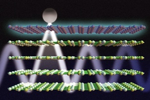 | |
| Researchers have shown that a DC voltage applied to layers of graphene and boron nitride can be used to control light emission from a nearby atom. Here, graphene is represented by a maroon-colored top layer; boron nitride is represented by yellow-green lattices below the graphene; and the atom is represented by a grey circle. A low concentration of DC voltage (in blue) allows the light to propagate inside the boron nitride, forming a tightly confined waveguide for optical signals. / Image: Anshuman Kumar Srivastava and Jose Luis Olivares/MIT |
The new findings - using a layer of one-atom-thick graphene deposited on top of a similar 2-D layer of a material called hexagonal boron nitride (hBN) - are published in the journal Nano Letters. The work is co-authored by MIT associate professor of mechanical engineering Nicholas Fang and graduate student Anshuman Kumar, and their co-authors at IBM's T.J. Watson Research Center, Hong Kong Polytechnic University, and the University of Minnesota.
Although the two materials are structurally similar - both composed of hexagonal arrays of atoms that form two-dimensional sheets - they each interact with light quite differently. But the researchers found that these interactions can be complementary, and can couple in ways that afford a great deal of control over the behavior of light.
The hybrid material blocks light when a particular voltage is applied to the graphene, while allowing a special kind of emission and propagation, called ''hyperbolicity,'' when a different voltage is applied - a phenomenon not seen before in optical systems, Fang says.
One of the consequences of this unusual behaviour is that an extremely thin sheet of material can interact strongly with light, allowing beams to be guided, funnelled, and controlled by voltages applied to the sheet.
''This poses a new opportunity to send and receive light over a very confined space,'' Fang says, and could lead to ''unique optical material that has great potential for optical interconnects.''
Many researchers see improved interconnection of optical and electronic components as a path to more efficient computation and imaging systems.
Light's interaction with graphene produces particles called plasmons, while light interacting with hBN produces phonons. Fang and his colleagues found that when the materials are combined in a certain way, the plasmons and phonons can couple, producing a strong resonance.
The properties of the graphene allow precise control over light, while hBN provides very strong confinement and guidance of the light. Combining the two makes it possible to create new ''metamaterials'' that marry the advantages of both, the researchers say.
Phaedon Avouris, a researcher at IBM and co-author of the paper, says, ''The combination of these two materials provides a unique system that allows the manipulation of optical processes.''
The combined materials create a tuned system that can be adjusted to allow light only of certain specific wavelengths or directions to propagate, they say. ''We can start to selectively pick some frequencies [to let through], and reject some,'' Kumar says.
These properties should make it possible, Fang says, to create tiny optical waveguides, about 20 nanometers in size - the same size range as the smallest features that can now be produced in microchips.
This could lead to chips that combine optical and electronic components in a single device, with far lower losses than when such devices are made separately and then interconnected, they say.
Co-author Tony Low, a researcher at IBM and the University of Minnesota, says, ''Our work paves the way for using 2-D material heterostructures for engineering new optical properties on demand.''
Another potential application, Fang says, comes from the ability to switch a light beam on and off at the material's surface; because the material naturally works at near-infrared wavelengths, this could enable new avenues for infrared spectroscopy, he says. ''It could even enable single-molecule resolution,'' Fang says, of biomolecules placed on the hybrid material's surface.
Sheng Shen, an assistant professor of mechanical engineering at Carnegie Mellon University who was not involved in this research, says, ''This work represents significant progress on understanding tunable interactions of light in graphene-hBN.''
The work is ''pretty critical'' for providing the understanding needed to develop optoelectronic or photonic devices based on graphene and hBN, he says, and ''could provide direct theoretical guidance on designing such types of devices. … I am personally very excited about this novel theoretical work.''
The research team also included Kin Hung Fung of Hong Kong Polytechnic University. The work was supported by the National Science Foundation and the Air Force Office of Scientific Research.