Performance boost for microchips
10 May 2012
The semiconductor industry is faced with the challenge of supplying ever faster and more powerful chips. The Next-Generation Lithography with EUV radiation, for which Fraunhofer researchers have developed key components, will help meeting that challenge.
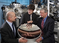 |
| CAPTION: Jointly developed key components for EUV lithography: Dr. Torsten Feigl, Dr. Stefan Braun and Dr. Klaus Bergmann (from left to right) with a collector mirror. © Dirk Mahler / Fraunhofer |
The microchips in today's computers already contain some two billion transistors. To get the chip density right, the structures are exposed onto the chips by means of lithography. To be able to meet future requirements, the semi-conductor industry is planning to convert the exposure using a wavelength of 193 nm to a wavelength of just 13.5 nm.
This can be achieved only with completely new radiation sources. The favourite of the Next-Generation lithography is EUV – light with wavelengths in the extreme ultraviolet range.
Dr Klaus Bergmann, Dr. Stefan Braun and Dr. Torsten Feigl from the Fraunhofer Institutes for Laser Technology ILT Aachen, for Material and Beam Technology IWS Dresden and for Applied Optics and Precision Engineering IOF Jena, have developed, with their teams, key elements for EUV lithography: light sources (ILT), collector optics (IOF) and illumination and projection optics (IWS). They will receive a 2012 Joseph-von-Fraunhofer prize for their achievements in this strategic partnership.
The efficiency of the light source is key to the industrial use of EUV. The team around Klaus Bergmann at ILT developed the first prototypes of the EUV source as early as 2006.
There is now a beta version that is already being used to expose chips in industrial applications. ''The concept is based on the rapid, pulsed discharge of electrically stored energy. In the process, a small amount of tin is vapourised using a laser and excited with a high current to an emission at 13.5 nm – many thousands of times per second'', explains Bergmann.
The quality of the collector mirror is crucial to the radiation hitting the exposure mask in exactly the right place. The coating guarantees that the losses remain low and that the quality of the focused EUV radiation is high.
''The challenge we faced was to develop and apply a multilayer coating system that combined high EUV reflectance with high thermal and radiation stability onto the strongly curved collector surface'', said Torsten Feigl from IOF. The result is the world's largest multi-layer coated EUV mirror with a diameter of more than 660 millimeters.
Once the radiation passed the mask, it is exposed onto the chips via further projection mirrors. Stefan Braun and his team at IWS have devised the optimum reflection layer for these components. Magnetron sputtering ensures maximum layer accuracy, without additional polishing processes or in-situ thickness control being required. One machine type for large area precision coating is already in industrial use.
Germany is the pioneer of EUV technology. Three institutes have established themselves with their research work as key partners for the supplier industry both in and outside Europe. The new lithography technology is expected to start industrial production in 2015.