‘Strained silicon’ nanowires may boost computing power
08 Jan 2010
Computers keep getting more powerful because silicon transistors keep getting smaller. But that miniaturization can't continue much further without a change to the transistors' design, which has remained more or less the same for 40 years.
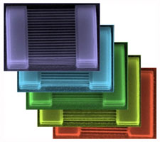 |
| Five different test structures feature stacks of nanowires with different numbers of levels. The bottom structure has only one level; the top structure has five. Images: Judy Hoyt, Pouya Hashemi and Leonardo Gomez |
A transistor is basically a switch: when it's on, it passes an electrical current, and when it's off, it doesn't. Flipping the switch requires charging a part of the transistor called the ''gate.'' In today's design, the gate sits on top of the transistor. But if the transistor gets small enough, electricity will leak across it whether the gate is charged or not. Turning the switch off becomes impossible.
Because silicon nanowires are suspended in air, the gate can be wrapped all the way around them, like insulation around an electrical wire, which improves control of the switch. But the narrowness of the nanowires limits the amount of current they can pass.
Electrical-engineering professor Judy Hoyt and her graduate students Pouya Hashemi and Leonardo Gomez improved the performance of silicon-nanowire transistors by, basically, prying the atoms of the silicon slightly farther apart than they would be naturally, which allows electrons to flow through the wires more freely. Such ''strained silicon'' has been a standard way to improve the performance of conventional transistors since 2003. But Hoyt was one of the early researchers in the field.
''Starting in the early 1990s, she's really played a pioneering role in strained-silicon technology,'' says Tahir Ghani, director of transistor technology and integration for Intel's Technology and Manufacturing Group. ''She did a lot of this pioneering work that for the first time demonstrated that you can have significant performance gains by implementing strain into silicon technology.'' Hoyt and her group's work on strained-silicon nanowires, Ghani says, ''combines the two key elements of transistors'' - performance and space efficiency - ''both of which are very key to scaling in the future. And so from that standpoint, it makes it very relevant for industry.''