Revolutionary semiconductor material from Motorola
05 September 2001
 Scientists at the Motorola Laboratories, which serves as the advanced research arm of the Motorola Inc., focusing on leading edge technologies for future products and product enhancements, have solved a problem that was vexing the semiconductor industry for the last thirty years. This discovery paves the way to transform the economics of the communications and semiconductor industries.
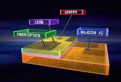
Motorola scientists have successfully combined the best properties of the workhorse silicon technology with the speed and optical capabilities of high-performance compound semiconductors that are known as the III-V materials.
The discovery opens the door to significantly less expensive optical communications, high-frequency radio devices and high-speed microprocessor-based subsystems by potentially eliminating the current cost barriers holding back many advanced applications.
The greatest beneficiaries are the consumers who should be able to get smarter electronic products that cost less, perform better and have exciting new features. It is expected that the new technology will change the economics and accelerate the development of new applications, such as broadband "fibre" cable to the home, streaming video to cell phones and automotive collision avoidance systems.
According to scientists at the Labs, other potential markets include data storage, lasers for such consumer products as DVD players, medical equipment, radar, automotive electronics, lighting, and photovoltaics. Until now, there has been no way to combine light-emitting semiconductors with silicon integrated circuits on a single chip, and the need to use discrete components has compromised the cost, size, speed and efficiency of high-speed communications equipment and devices.
Motorola's announcement specifically impacts the semiconductor industry by:
- increasing substrate size, reducing substrate cost and processing costs for III-V manufacturing
- integrating the superior electrical and optical performance of III-V semiconductors with mature silicon technology to create a new industry based on integrated semiconductor circuits
- extending the life of silicon and existing capital investments
- improving cost effectiveness for higher performance applications such as optical communications Enabling larger scales of integration
Terming this as one of the most significant achievements of recent years, Dennis Robertson, senior vice president and chief technology officer of Motorola said that, when fully commercialised, this discovery would transform the industry in a way that is similar to the transition from discrete semiconductors to integrated circuits.
Several industry experts have stated that this discovery could well be the turning point for the semiconductor industry.
The Technology
Until now it has been virtually impossible to grow semiconductor materials on a silicon substrate. The discovery by Motorola enables very thin layers of so-called III-V semiconductor materials (which include gallium arsenide, indium phosphide, gallium nitride and other high performance / light-emitting compounds) to be grown on a silicon substrate.
